
Microstructural analysis
Why do we need microscopy to study 3D printed parts?
The main challenge currently with additive manufacturing (AM) of metal is the lack of scientific understanding of the underlying processes that lead to complex microstructures and property relationships.
Without a strong understanding of these processes it is impossible to eliminate uncertainties in the 3D printing process, which can cause internal stresses within the part, leading to deformation or even catastrophic failure.
In order to rely on parts that are being built, it is essential that the influence of different printing parameters is investigated in more detail. This can be achieved by using different analysis techniques that yield information at the macro-, micro- and nano scale.
The following section gives a brief overview of some of the microscopy techniques that can be used for microstructural analysis. It is an introduction only and for more details on operating principles please click here.
Optical Microscopy
To study macrostructures, an optical microscope is the ideal tool for primary visualisation, as it is relatively easy to use and can yield a good overview of the sample surface and its features. It uses visible light, which has a wavelength ranging from 400 nm (violet) to 650 nm (red), and a system of lenses to magnify the sample. As for any microscope, the theoretical resolution limit is described by the Abbe diffraction limit, 𝑑=𝜆2𝑛 sin𝜃, where λ is the wavelength, n the refractive index and θ is angular aperture of the lens. According to this equation, the theoretical resolution limit of an optical microscope is around 200 nm, but this limit is almost never reached.
The main use for optical microscopy in the context of AM is to investigate melt pools (see image below), as their size and shape affect the resulting microstructure which in turn influences the mechanical properties of the printed part.
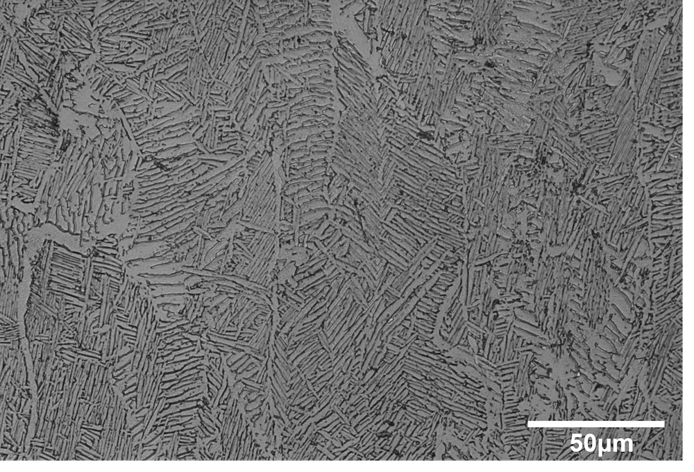
Figure 1: Optical microscopy image of an AM sample surface
Scanning Electron Microscopy (SEM)
Scanning Electron Microscopy (SEM) is an extremely useful surface imaging technique, as it can be used to study microstructural phenomena at much higher resolution than optical microscopy. at the micrometre and nanometre level. The higher spatial resolution, typically around 5 nm, is achieved through using an electron beam, which has a much smaller wavelength compared to the wavelength of visible light. A SEM creates a magnified image by scanning a focused electron beam over a sample and detecting secondary or back-scattered electrons (SE or BSE). The electron beam is focused and scanned across the specimen by a series of electromagnets, which act similar to glass lenses in a traditional optical microscope. A SE or BSE detector measures the incoming electrons at each point in the raster and the magnified image is displayed using a computer.
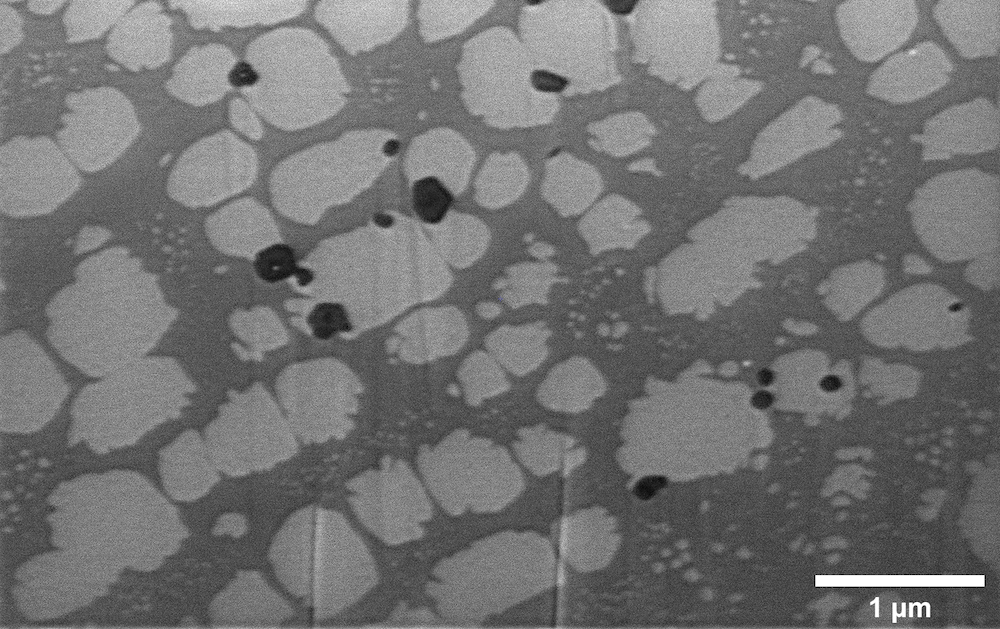
Figure 2: SEM image of an AM alloy
A SEM can be equipped with a focused ion beam (FIB), which can be used to cut small trenches or patterns into the sample, in order to observe and analyse the exposed areas of the material or to prepare samples for other analysis techniques such as transmission electron microscopy (TEM) and atom probe tomography (APT). Conventional FIBs typically use Ga+ions to mill and shape a sample. However, in recent years a FIB has been developed that uses a plasma beam for milling (P-FIB). Typical gas sources for the P-FIB are Xe (most common), Ar, N2 and O2. The P-FIB has the advantage that it has much faster milling rates, making it easier to remove large areas of material.
Often a SEM is equipped with various detectors, such as an electron backscatter diffraction (EBSD) detector, and/or an energy dispersive X-ray spectroscopy (EDS) detector. EBSD is a specialised SEM technique, which is used to investigate the structure, phase and crystal orientation of crystalline materials, and therefore an extremely valuable tool in the field of additive manufacturing. It can reveal texture, grain size and morphology, defects and deformation. To perform EBSD, the sample has to have an extremely well-polished surface, in order for to minimize surface topology and strain, which affects diffraction and creates artefacts.
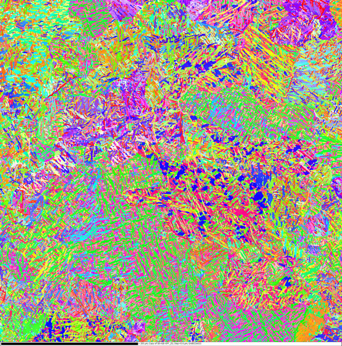
Figure 4: EBSD image of an AM alloy. The different colours represent different crystallographic orientations
If FIB and EBSD are combined, 3D EBSD can be performed, which allows for visualisation of a sample’s morphology in 3D. For this to work, a FIB is used to mill away a series of cross-sectional layers and after each layer an EBSD image is taken. Specialised software must be used to align and stitch together the set of 2D EBSD maps into the 3D representation.
Transmission Kikuchi Diffraction (TKD) is a modified form of EBSD, but in this case an electron transparent sample must be used, as the Kikuchi pattern is generated at the bottom of the sample rather than on the surface of the bulk material, as is the case for EBSD. Therefore, much better spatial resolution can be achieved – in some cases as low as 2 nm (depending on the SEM system used, sample quality and density).
Energy dispersive x-ray spectroscopy (EDS) is a technique used to investigate the elemental composition and chemical characteristics of a sample. When electrons from the electron beam enter the sample, x-rays – called characteristic x-rays – are emitted corresponding to the elements present in the sample. The energy of the characteristic x-rays are used to determine the elements present, and the relative intensity of the x-rays allows the concentrations to be quantified. By collecting EDS and EBSD data simultaneously, phases with similar crystal structure, which can’t be distinguished by EBSD data alone, can be distinguished based on chemical composition. Furthermore, both composition and structural information can be correlated.
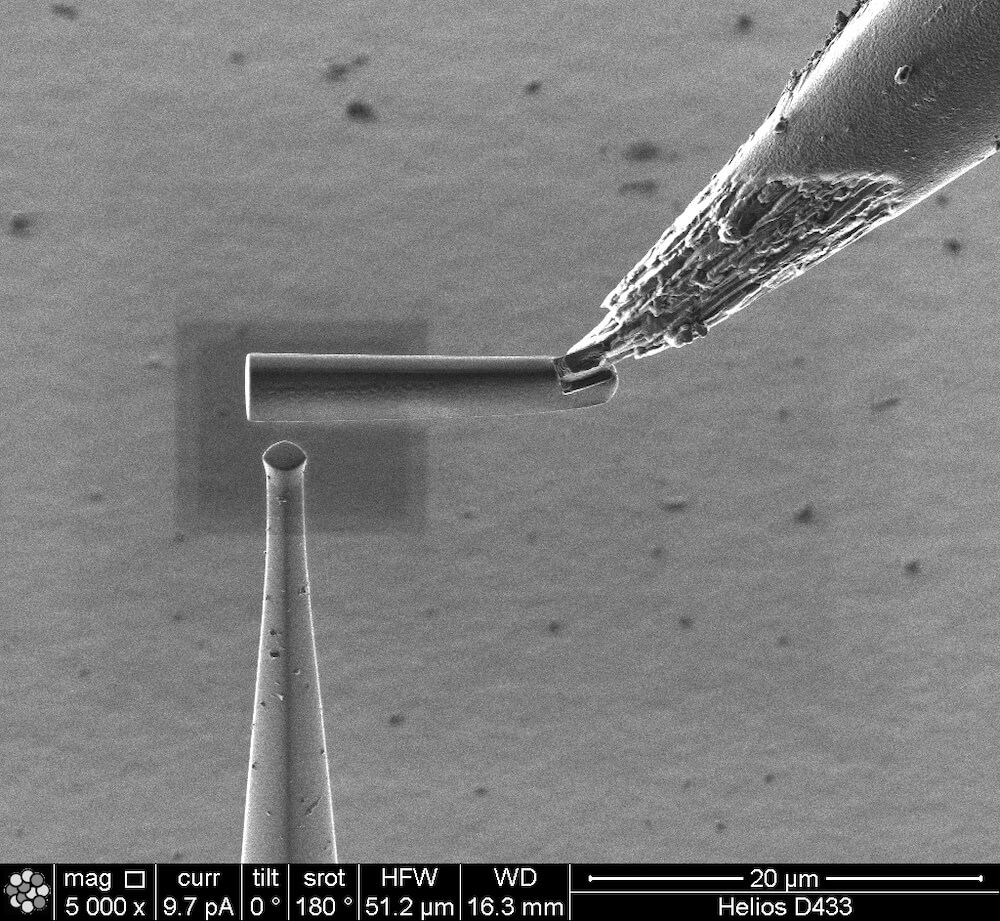
Figure 3: SEM image of a FIB lamella, attached to a micromanipulator
EDS can be used in SEM and TEM, as characteristic x-rays are emitted during both processes. For 3D printed alloys, EDS can be used to visualise how concentrations of one element varies over the sample, potentially showing partitioning and segregation of elements that influence the materials properties.
Transmission Electron Microscopy (TEM)
TEM is used to investigate microstructural features by passing a highly energetic electron beam through an electron transparent sample. TEM can produce high resolution images, with a resolution down to < 63 pm, for a state-of-the-art aberration corrected TEM.
Only ultra-thin samples with a thickness of less than 100 nm are suitable for high-resolution TEM investigations. The contrast of TEM images can be produced in many ways, such as thickness or density contrast, Z-contrast, and crystal structure or orientation with each image yielding different information.
Furthermore, various operating TEM modes can be used, including conventional imaging in bright field or dark field mode, scanning TEM imaging (STEM), diffraction, spectroscopy, as well as combinations of these. This makes TEM a very versatile analytical tool.
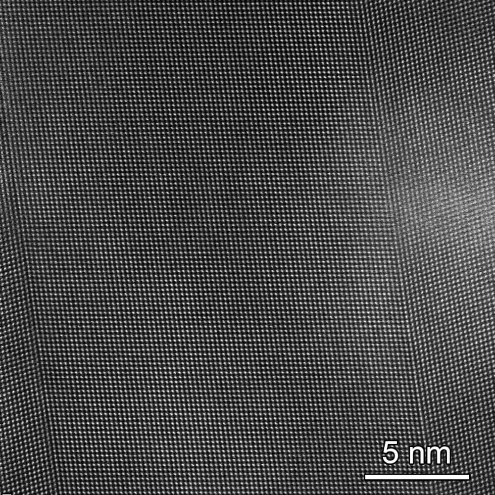
Figure 5: TEM image of an AM alloy
In-situ electron microscopy
Both SEM and TEM can be used to investigate the behaviour of a material in real-time when subjected to a stimuli such as heat or deformation. This allows for correlation of a sample’s microstructure and mechanical properties and can be extremely helpful when trying to predict a material’s behaviour in real-world applications.
Atom Probe Tomography (APT)
APT is an analysis technique that generates a 3D reconstruction of 10s of millions of individual atoms from a specimen, for volumes in the order of 105 – 106 nm2. APT can provide near-atomic resolution and high chemical sensitivity. Even light elements such as H, He and Li can be detected.
To perform APT, an ultra-sharp needle is prepared from a sample, either by conventional electrochemical polishing or, if a particular region-of-interest is required, by site-specific lift-out on a (P-)FIB. The radius of the needle tip is generally between 50 – 100 nm. Once inside the vacuum of the atom probe, a standing voltage is applied onto the sample. On top of the standing voltage, a voltage or laser pulse is applied to induce field ionisation.
Field evaporated atoms get removed from the specimen, atom by atom, layer by layer and hit a position sensitive detector. The time-of-flight of each detector hit is also recorded and used during the reconstruction process to determine the mass-to-charge-state-ratio and therefore the elemental identity of each detected ion.
Atom probe is a powerful tool to visualise and determine the local composition, location of grain boundaries, and also if and where precipitation, segregation or clustering of solutes occurs. Furthermore, it can provide information about the crystallographic structure of the specimen analysed.
Figure 6: APT reconstruction. Each sphere represents one detected atom, with the different colours being different elements